
The BBC and Master Computer Public Domain Library
Mapped Master 128
BBC Master 128
IC1
7406 (TTL Hex inverter)Used to buffer various signals from the Floppy Disc Controller IC3
IC2
7438 (TTL Quad 2-input NAND gate, open collector)IC3
WD1770 Floppy Disc ControllerIC4
74LS174 (TLL hex D-flipflop)IC5
74LS244 (TTL Octal Buffer)See IC6
IC6
6522 (Versatile Interface Adapter, VIA)IC6 is the second versatile interface adaptor present in the BBC Master 128. Port A is used to provide a centronics standard parallel printer interface, with the octal buffer IC5 being used to buffer the data lines. Port B is left uncommitted and is free for use by the user for input or output purposes. For a functional description of the VIA, see IC8.
IC7
74LS373IC8
6522 (Versatile Interface Adapter, VIA)A VIA has two sets of 8 I/O lines with two associated control lines, known as Ports A and B. Each I/O line can be set to input or output individually using the VIA's Data Direction registers; the control lines (CA1/CA2, CB1/CB2) act as handshake signals for their respective ports. The input and output registers are latched. Each VIA also contains two 16-bit programmable timer/counters and a shift register.
The BBC Master contains two VIAs. One (IC8) is dedicated to internal system operation, the other (IC6) provides the printer interface and the user port (PL4).
Port A of the system VIA acts as a slow data bus which connects to the keyboard and its encoder, the sound generator (IC12) and the system Real Time Clock (IC11). Port B drives an addressable latch (IC10) which is used to provide read and write strobe signals for the RTC, the keyboard and the sound generator chip. Also, coming from this latch are control lines C0 and C1 which indicate the amount of RAM devoted to the display memory to be 16K, 8K, 10K or 20K. Outputs 6 and 7 of the addressable latch drive the caps lock and shift lock LEDs on the keyboard. Two I/O lines on Port B are used to input the two 'fire button' signals from the game connector SK6 and two more lines are used controlling the RTC. Each time the system VIA is written to, the latch connected to port B is strobed by a flipflop which is triggered from the 1MHz clock signal. Port A control line 1 (CA1) is used for detecting keyboard activity, CA2 is connected to the video vertical sync, to generate the Start of Vertical Sync event. CB1 takes the ADC End Of Conversion signal, and CB2 is used for the Light Pen Strobe signal.
IC9
LM324 QUAD 0P AMPSee IC12.
IC10
74LS259 (TTL 3-to-8 decoder/latch)See IC8
IC11
146818 RTC CM0SThis chip contains the Master's Real Time Clock, and also provides 50 bytes worth of RAM storage for various system parameters such as the default serial baud rate, video mode and similar settings. When the system is switched off it is powered by a 4.5V battery pack connected to PL8, thus allowing the clock to keep running and providing non-volatile storage.
IC12
76489 S0UND GENERATORIC12 is a four channel sound generator chip which may be programmed to generate sounds of varying frequency and amplitude on each channel. A quad opamp (IC9) performs mixing the sound generator and the optional modem and speech generator signals, amplifies and filters the result, and feeds it to IC13.
IC13
LM386 AUDIO AMPIC13 provides audio power amplification to drive a speaker (connected to SK13).
IC14
65C12 CPU CM0S 2MHZThe microprocessor used in the BBC Master is a 65C12A running at 2MHz. The 65C12 CPU is essentially a CMOS version of the 6502 CPU used in the original BBC models, with some minor technical changes to the clock circuitry and the data I/O lines.
A 16MHz crystal oscillator is used to provide clock signals for the CPU in conjunction with divider circuitry in the video processor ULA (IC42) which produces 8, 4, 2 and 1 MHz signals. The 1MHz system clock is actually generated by clocking the 1MHz signal out of the ULA through a D-flipflop (half of IC28); the 1MHz signal out of the video ULA is not used anywhere else. Switching the CPU down to 1MHz from the 2MHz it's normally running at when accessing a slow peripheral, as required in the A, B and B+ models, doesn't happen in the Master. Instead, the PBC takes care of this, dividing the bus into fast and slow sections.
IC15
MSI I/0 Controller (CF30050)This custom IC performs the address decoding for the various peripherals present in the BBC Master: the CRT controller, the ACIA and serial ULA, floppy controller, both VIAs, the ADC, Tube and 1MHz bus.
IC16
MSI Keyboard Encoder (CF30047)IC17,18,23,26
4464 DRAM 120nS 64Kx4Random Access Memory on the Master is provided by 4 dynamic memory devices (DRAM) (ICs 17, 18, 23 and 26).
In order to reduce the external pin count and simplify the internal architecture of DRAM devices, their address inputs are usually multiplexed. The 256kbit devices (64k addresses, 4 bit wide) used in the BBC Master require 16 address lines, but by virtue of this multiplexing only 8 pins are required. Addressing is achieved by first offering the lower 8 bits of the address which are then latched by the DRAM on a Row Address Strobe (RAS) signal, after which the high 8 bits of the address are set up and latched by a Column Address Strobe (CAS) signal. At this point the required address is complete, and data can be read or written. This sounds like a time-consuming process, but by running the address multiplexing at twice the speed of the address bus clock the DRAM data stays in step with the rest of the system.
In the Master, the RAS and CAS signals are generated from the 8, 4 and 2
MHz clock signals by the video memory mapper IC31,
and part of ICs 34 and 38.
Two devices may have control of the RAM address lines: the 65C12 CPU
(IC14) and the 6845 CRTC (IC22).
The CRTC generates the raster scan signals for the video display,
together with the address for each memory mapped byte of information in
the RAMs which is required to refresh the display. Selecting which of
these two devices control the DRAM address lines is done through IC31, and ICs 29, 30 and 33.
The 128kB RAM fitted in the BBC Master is split into three banks. One is mapped to the range &0000-&AFFF, another to &3000-&7FFF. The remaining memory can be used as Sideways RAM, acting as a Language ROM which can be loaded on-the-fly. The second bank (&3000-&7FFF) can only be used as screen memory, and only when "shadow mode" is enabled. As shadow screen memory it is not directly accessible from a program running in "normal" memory, instead requiring bank switching. Programs that manipulate video by reading or writing screen memory directly will not work with shadow mode video screens; all video memory reads and writes have to go through the OS. The advantage of shadow screen memory comes from having 32kB RAM available to user programs, independently of the video mode selected. Shadow memory switching is done largely by the Memory Switch IC20.
IC19
74LS14 (TTL hex inverter/Schmitt trigger)IC20
MSI Memory Switch (CF30058)Custom gate array performing the various bank switching tasks pertaining to the system and language ROMs, sideways RAM, and shadow video memory.
IC21
MSI Peripheral Bus Controller (CF30049)Custom gate array, designed to split the system's data bus into three sections. This is to reduce output loading on any active device from inactive devices, as well as separating slow (1MHz) peripherals from the fast (2MHz) CPU bus. The three sections comprise:
- CPU, ROM and RAM memory, internal Tube, Econet.
- CRTC, SAA5050 and video ULA, 6850 and serial ULA, FDC, both VIAs and the ADC.
- External Tube and 1MHz bus.
IC22
6845 (CRT controller, CRTC)This is the heart of the BBC Master's video circuitry. Its major function is that of displaying the video data in memory on a raster scan display device such as a television or monitor. As a bonus, the sequential nature of accessing the system RAM for the video display refreshes all the DRAM storage.
The CRTC does not interfere with CPU access to the memory, as they operate on alternate phases of the system clock.
The 6845 is responsible for producing the correct format on the display device, positioning the cursor, and monitoring the light pen input. Other video functions involving colour and Teletext are dealt with by the video ULA (IC42) and the Teletext Character Generator (IC32).
IC24
MOS 1MB ROMApart from the OS/DFS/BASIC ROM, three other ROMs (ICs 27, 37 and 41) can be on the main circuit board.
Overall address decoding for the ROMs is by the I/O controller (IC15). The operating system occupies the address range &C000-&FFFF; the address range &8000-&BFFF can be occupied by one of several 16kB-sections of the MOS ROM, or one of the installed additional ROMs by means of 'bank switching'. This allows for different programming languages, system software extensions such as a Network Filing System, or application software like a word processor to be installed, and be activated when needed. The OS and BASIC are contained in one physical ROM, but the bank switching treats the range &8000-&BFFF as logically identical to any of the additional ROMs.
. Each of the auxiliary sockets can contain 8kB, 16kB or 32kB devices, where the latter are treated as two 16kB devices.
Two of the sockets can be disabled, and Sideways RAM selected to appear in the bank switching slots they occupy, via two jumpers. This allows languages, tools or system extensions to be loaded when needed, while still being treated as if they were installed as ROMs.
IC25
74LS86 (TTL quad 2-input EXOR gate)IC27
28-pin IC socketIC28
74F74 (TLL dual D-flipflop)IC29, IC33
74HCT253 (TTL dual 4-input multiplexer, tri-state output)Used in multiplexing the DRAM address lines.
IC30
74LS257 (TTL quad 2-input multiplexer, tri-state output)Used in multiplexing the DRAM address lines.
IC31
MSI CRTC Multiplexer (CF30048)Custom gate array performing the mapping of the CRTC's address lines on to the right area of the system DRAM depending on the video mode, and simultaneously multiplexing the address lines.
IC32
SAA5050 (Teletext Character Generator)Display modes 7 and 135 are Teletext character modes. When using this mode, only 1K of RAM is devoted to the display memory and the characters are held within it as ASCII bytes. To implement this an SAA5050 Teletext character generator is used. IC15 latches the DRAM data going into the SAA5050, which then translates these bytes into a standard Teletext/Prestel format display.
A 6MHz clock signal is required for the operation of this device. This signal is produced by knocking a reset flip flop (two quarters of IC39) backwards and forwards from 8MHz and 4MHz clock signals. The resulting flip flop output is then itself inverted according to the state of the 2MHz clock signal by an exclusive OR gate (.25 of IC25). Glitches on this output are removed by R59 and C30 to produce the 6MHz clock signal at IC25 pin 11.
IC34
74S00 (TLL quad 2-input NAND gate)IC35
Not fittedIC36
74F00 (TTL quad 2-input NAND gate)IC37
28-pin IC socketIC38
74LS00 (TTL quad 2-input NAND gate)IC39
74LS02 (TTL quad 2-input NOR gate)IC40
MSI Chroma generator (CF30060)Custom gate array used for mixing the separate red, green and blue signals from the video ULA (IC42) into a composite signal, and adding a colour burst reference.
IC41
28-pin IC socketIC42
VC2069 VIDEO ULAThe video processor device (IC42) is a custom uncommitted logic array (ULA) based on the 5C094 ULA developed especially for use in the BBC Micro. At the end of each CRTC 250nS access period, it latches the byte from the RAM and, according to the display mode in operation, serialises the byte into 1 bit stream of 8 bits or 2 bit streams of 4 bits etc. In this way, display modes varying in width from 640 pixels in 2 colours to 160 pixels in 8 colours, which may or may not be flashing, can be produced. Also, in the video processor is a high speed piece of static RAM called a palette. This memory can be programmed to define the relationship between the logical colour produced by the RAM and the physical colour which will appear on the display. Thus, in a 640 pixel mode, the two colours to appear on the display need not be black and white, they may be, say, red and blue. Note that the data in RAM is unchanged by the palette, it is the mapping onto physical colours which changes.
Modes 0 through 6 in the Master are so-called bitmapped screens, which allow for raster graphics. With these screens, each pixel on the screen corresponds directly with one, two or four bits in the video memory. This method of producing video screens is expensive in memory, involving a minimum of 8 kilobytes for the display.
IC43
74S04 (TTL hex inverter)IC45
6850 (Asynchronous Communication Interface Adapter, ACIA)This device is used to buffer and serialise or deserialise the RS423 and cassette data. It is used in conjunction with an Uncommited Logic Array (ULA) (IC48) initially designed for the BBC Micro, and subsequently used in later models like the B+ and, with slight modifications, the Master.
Contained within this ULA is a programmable baud rate generator, a cassette data/clock separator and switching to select either RS423 or cassette operations. IC42 divides the main board 16MHz clock by 13 and this signal is divided further within the serial interface ULA to produce the 1200 Hz cassette signal. Automatic motor control of an audio cassette recorder is achieved by a small relay driven by a transistor from the serial interface ULA. The signal out of the cassette is buffered and the incoming signal is suitably filtered and shaped by a three stage amplifier, implemented using a LM324 quad opamp (IC46).
IC46
LM324 QUAD 0P AMPSee IC45
IC48
VC2026 Serial ULASee IC45
IC49
uPD7002 (Analogue to Digital Converter, ADC)This device provides a four channel ADC facility with 10-bit resolution. It connects straight to the Master's data bus and is a dual slope convertor with its voltage reference being provided by the three diodes D17, D18 and D19.
IC50
3691 RS422/423 DriverThe RS423 Transmit and Receive data signals and the Request-To-Send and Clear-To-Send flow control signals are interfaced by ICs 50 and 51 which translate between TTL and standard RS423/232 signal levels. Note that this is one of the few sections of circuitry on the Master which requires an additional -5v supply to be present.
IC51
9637A RS422/423 ReceiverSee IC50
Keyboard
General description:- 93 keys are provided. 92 of these are in a modified 8 x 13 matrix as shown in figure 5. A keyboard encoder, IC16 is used to scan the keyboard. During idle (free run) mode, pressing any key will cause an IRQ to be generated via the system VIA. A connection is provided from IC16 to the VIA's 'CA' input. Hence the interrupts thus generated are controlled by the 6522 control register. Depression of either of the shift keys, or the control key does not cause an interrupt to occur.
Keys are arranged as a QWERTY style keyboard with extra keys for a
numeric keypad. Ten additional 'function keys' together with cursor
control buttons, etc., are provided.
The "BREAK" key will reset the CPU and abort any access to the clock/RAM
chip. To prevent accidental operation, a mechanical lock is provided. This
is a plastic cam which is rotated through 90 degrees to stop the keytop
from being depressed.
Keyboard Operation:- During free run mode, the keyboard column lines
are continually scanned by incrementing a counter, decoding its outputs
and pulling low a column line. Any key depressed will cause the interrupt
to be generated. A signal, KeyBoard ENable is generated to stop free running
mode. The counter contents are now loaded by CPU operation to determine
on which row the key was pressed. The rows are then individually selected
to determine which key was pressed.
LK12
3w WAFR 0.1 ST PCBPlug, made B (East): CSYNC/Cartridge Machine Detect.
Two position link.
- Position A - This connection to the computer CSYNC line is provided for GENLOCK purposes.
- Position B - Certain hardware cartridges may need to detect whether they are plugged into a Master Series computer or an Acorn Electron. Master computers are shipped with this link in the B position, causing a logic LOW to appear on pin A10 of the cartridges. The Electron has no connection to this pin.
LK18
3w WAFR 0.1 ST PCBplug, made West: Paged ROM/RAM Select.
Two position link.
- When fitted in the West position, this link causes 16Kbyte of RAM to appear in each of the "sideways" memory "slots" 6 and 7.
- When fitted in the East position, a 32Kbyte ROM occupying slots 6 and 7 may be plugged into socket labelled IC41.
LK19
3w WAFR 0.1 ST PCBplug, made West: Paged ROM/RAM Select.
Two position link.
- When fitted in the West position, this link causes 16Kbyte of RAM to appear in each of the "sideways" memory "slots" 4 and 5.
- When fitted in the East position, a 32Kbyte ROM occupying slots 4 and 5 may be plugged into socket labelled IC37.
MD1
UM1233 UHF PAL Modulator WB E36PAL/NTSC encoded, UHF carrier On channel 36 with 1.5mV into 75 ohm.
For use with NTSC, the modulator has to be changed from UM1233/E36
to a VHF equivalent. Provision is made for selection of either one of two
channels with VHF. A Molex type link has to be inserted for this.
PSU
The power supply unit is connected to the main circuit board by seven push-on connectors which must be unplugged. Three screws on the underside of the case are undone allowing the unit to be removed. On reassembly, ensure that the same type of screw is used (M3x6mm).
IDC Connectors
All IDC connector pins are numbered in this way:
PL1,PL2
Disc Drive Connectors34way IDC header
| signal | pin | pin | signal |
|---|---|---|---|
| 0V | 1 | 2 | (notSSEL 8") |
| 0V | 3 | 4 | (notINX 8") |
| 0V | 5 | 6 | NC |
| 0V | 7 | 8 | notINX 5 1/4" |
| 0V | 9 | 10 | notS0 |
| 0V | 11 | 12 | notS1 |
| 0V | 13 | 14 | NC |
| 0V | 15 | 16 | notMOTOR |
| 0V | 17 | 18 | notDIR |
| 0V | 19 | 20 | notSTEP |
| 0V | 21 | 22 | notW/DATA |
| 0V | 23 | 24 | notWR/EN |
| 0V | 25 | 26 | notTK0 |
| 0V | 27 | 28 | notWR PCT |
| 0V | 29 | 30 | notR/DATA |
| 0V | 31 | 32 | notS/SEL 5 1/4" |
| 0V | 33 | 34 | (notRDY 8") |
PL3
Printer Connector26way IDC header
| signal | pin | pin | signal |
|---|---|---|---|
| STB | 1 | 2 | 0V |
| PA0 | 3 | 4 | 0V |
| PA1 | 5 | 6 | 0V |
| PA2 | 7 | 8 | 0V |
| PA3 | 9 | 10 | 0V |
| PA4 | 11 | 12 | 0V |
| PA5 | 13 | 14 | 0V |
| PA6 | 15 | 16 | 0V |
| PA7 | 17 | 18 | 0V |
| ACK | 19 | 20 | 0V |
| NC | 21 | 22 | 0V |
| NC | 23 | 24 | 0V |
| NC | 25 | 26 | NC |
PL4
User Port Connector20way IDC header
| signal | pin | pin | signal |
|---|---|---|---|
| +5V | 1 | 2 | CB1 |
| +5V | 3 | 4 | CB2 |
| 0V | 5 | 6 | PB0 |
| 0V | 7 | 8 | PB1 |
| 0V | 9 | 10 | PB2 |
| 0V | 11 | 12 | PB3 |
| 0V | 13 | 14 | PB4 |
| 0V | 15 | 16 | PB5 |
| 0V | 17 | 18 | PB6 |
| 0V | 19 | 20 | PB7 |
PL5
1MHz Bus Connector34way IDC header
| signal | pin | pin | signal |
|---|---|---|---|
| 0V | 1 | 2 | R/notW |
| 0V | 3 | 4 | 1MHzE |
| 0V | 5 | 6 | notNMI |
| 0V | 7 | 8 | notIRQ |
| 0V | 9 | 10 | notPGFC |
| 0V | 11 | 12 | notPGFD |
| 0V | 13 | 14 | notRESET |
| 0V | 15 | 16 | audio in/out (see LK1) |
| 0V | 17 | 18 | D0 |
| D1 | 19 | 20 | D2 |
| D3 | 21 | 22 | D4 |
| D5 | 23 | 24 | D6 |
| D7 | 25 | 26 | 0V |
| A0 | 27 | 28 | A1 |
| A2 | 29 | 30 | A3 |
| A4 | 31 | 32 | A5 |
| A6 | 33 | 34 | A7 |
PL6
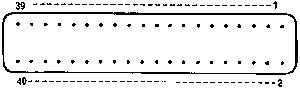
Tube Connector40way IDC header
| signal | pin | pin | signal |
|---|---|---|---|
| 0V | 1 | 2 | R/notW |
| 0V | 3 | 4 | 2MHzE |
| 0V | 5 | 6 | notIRQ |
| 0V | 7 | 8 | notTUBE |
| 0V | 9 | 10 | notRESET |
| 0V | 11 | 12 | D0 |
| 0V | 13 | 14 | D1 |
| 0V | 15 | 16 | D2 |
| 0V | 17 | 18 | D3 |
| 0V | 19 | 20 | D4 |
| 0V | 21 | 22 | D5 |
| 0V | 23 | 24 | D6 |
| 0V | 25 | 26 | D7 |
| 0V | 27 | 28 | A0 |
| 0V | 29 | 30 | A1 |
| +5V | 31 | 32 | A2 |
| +5V | 33 | 34 | A3 |
| +5V | 35 | 36 | A4 |
| +5V | 37 | 38 | NC |
| +5V | 39 | 40 | NC |
PL8
3w WAFR 0.1 ST PCBPL9
2W WAFR .1 RA PCBPL10
5W WAFR 0.1'' RA 11PINPL17,PL19,PL21
TAB 6.3mm ST PCB+5V supply
PL18,PL20,PL22
TAB 6.3mm ST PCBsupply ground
PL23
TAB 6.3mm ST PCB-5V supply
RL1
RLY 1P C0 5V 50R PCBCassette Relay
SK1
12Way socketExpansion Board Slot/Internal Tube connector
SK2
12Way socketExpansion Board Slot/Internal Tube connector
SK3,SK4
Cartridge SlotsSK5
19w SKT HSNG 0.1 PCBEconet Board Slot (system bus connector)
SK6
5W SKT HSNG 0.1 PCBEconet Board Slot (I/O connector)
SK7
5W SKT DIN RA PCBEconet Din Plug
SK8
BNC SKT 75R PNLBNC Video Out connector
SK9
6w SKT DIN RA PCBRGB video out connector
SK10
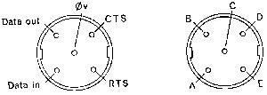
5W SKT DIN RA D0MRS423 connector
SK11
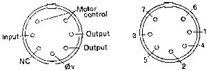
7w SKT DIN RA PCBCassette connector
SK12
Analogue In Connector15W SKT D
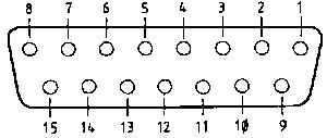
| pin | signal |
|---|---|
| 1 | +5V |
| 2 | 0V |
| 3 | 0V |
| 4 | CH3 |
| 5 | analogue ground |
| 6 | 0V |
| 7 | CH1 |
| 8 | analogue ground |
| 9 | light pen strobe (notLPSTB) |
| 10 | digital switch input (I1) |
| 11 | voltage reference (VREF) |
| 12 | CH2 |
| 13 | digital switch input (I0) |
| 14 | voltage reference (VREF) |
| 15 | CH0 |
SK13
PHONO SKT RA PCBAudio Out